 2022/11/04
一、Background knowledge
The use of machine vision in the production of semiconductor materials industry has begun for a long time. Driven by the increasing popularity of large-scale electronic devices in the production of semiconductor materials industry, the demand for production volume and the pursuit of product quality in the field are increasing. Machine vision technology plays an indispensable role, and the demand for machine vision technology continues to break the old and establish the new.Machine vision itself is also developing and improving with the rapid development of semiconductor, electronics, automation, optics and other skills.

What are the applications of machine vision in the semiconductor industry?
1. Application in appearance inspection of small and medium-sized electronic components and small-sized industrial products, appearance inspection of SMD products, and appearance inspection of monocrystalline silicon wafers. The inspection contents include hot stamping, content, image, orientation error, etc., or missing printing, surface defects, etc. After the surface of the measured object is quickly and automatically photographed, the data is transmitted to the computer to solve the problem, and fake and inferior products are found.
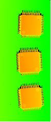
2. Application in flatness detection of IC chip and electronic device connector Check the number of pins and the number of specifications of several parts of the pins, including pitch, total width, relative height and bending degree.The continuous, efficient and rapid appearance inspection of the integrated IC is completed, the inspection efficiency is improved, the labor cost is saved, the labor efficiency of workers is reduced, and more importantly, the inspection precision is ensured.
3. PCB printed circuit board detection, board component position, solder joint, circuit, punching specification, angle measurement; micro-communication interface on the computer, SIM card memory slot; SMT component placement, surface patch, surface detection; SPI solder paste detection, reflow soldering furnace and wave soldering machine; detection and accurate measurement of the number of cable connectors.
II. Application of LVM Line Laser Products in Semiconductor Industry
1. PCB glue path detection: The 3D sensor generates a height map by scanning PCB materials to detect the glue height and width.
1) Customer requirements
The PCB glue path is detected, and the glue height and width are measured.
2) Detection method and equipment
Test camera: LVM-2520
Scanning interval: 0.032 mm
Sensor frequency: 7000HZ
Working distance: 51 ± 5mm
Scanning mode: camera fixed, workpiece moving
3) Map acquisition effect
Horizontal product point cloud effect:
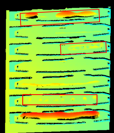
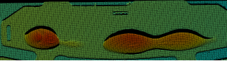


Vertical product point cloud effect:
Vertical product point cloud effect:

4) Test data
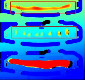
Test data of glue height:
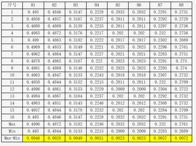
Note: The results of glue height measurement data are shown in the figure above.
l Measurement method: Take a certain area on the board as the reference plane, and calculate the height difference between 8 glue points and the reference plane;
l The 16 times dynamic repeatability data of 8 glue spots are all within 7.5 um.
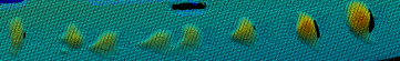
Rubber width test data:
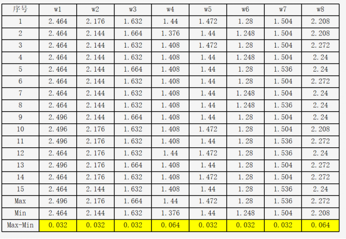
Note: The results of glue width measurement data are shown in the figure above:
l Measurement method: measure the minimum circumscribed rectangle of the product
l The 16 times dynamic repeatability data of 8 glue spots are all within 0.064 mm.
l Because the product is in an irregular state, it is impossible to extract valid edges using the conventional edge extraction method.
5) Summary
|
Customer samples |
Type of test |
Conclusion |
|
PCB dispensing |
Scanning mode |
Vertical scanning has more noise than horizontal scanning point cloud data, and the maximum scanning speed is 200mm/s, which can meet the customer's CT needs. |
|
Glue height |
Dynamic repeatability within 0.01 mm |
|
|
Rubber width |
Dynamic repeatability within 0.065 mm |
Note: Pay attention to the blind area during feature scanning, but the blind area cannot be the highest point of the rubber path.
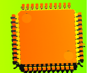
2. Component PIN height difference detection: The 3D sensor generates a height map by scanning the component PIN, and measures the height difference between the PIN and the bottom surface.
1) Customer requirements
Height difference detection of PIN pin of components and parts, accuracy requirement 0.005 ~ 0.008 mm, CT requirement 200mm/s.
2) Detection method and equipment
Test camera: LVM-2520
FOV:28.1mm-38.6mm
X-direction resolution: 14-20 um
Depth of field: 24.3mm
Repeatability in Z direction: 0.5 um
Scanning mode: fixed camera and moving workpiece
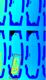
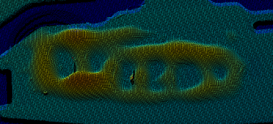
3) Map acquisition effect
Original point cloud effect:
Example of the effect after treatment:
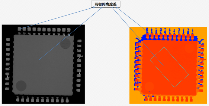
4) Test results
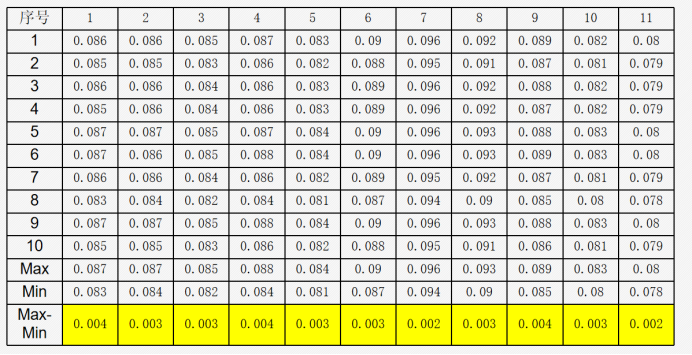
Note: 11 PIN needles in the upper row were tested, and the data were scanned statically for ten times, with the maximum repeatability of 0.004 mm and the minimum repeatability of 0.002 mm.
About Us
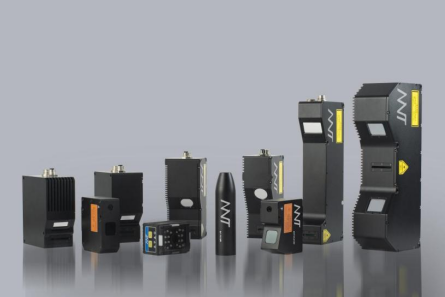
Founded in 2017, Next Vision Tech is a high-tech enterprise integrating industrial visual product design, research and development, production, sales and service. The company focuses on the underlying algorithm development and hardware implementation of industrial vision products, and has a complete set of software and hardware technologies with independent intellectual property rights. The goal is to become the world's leading vision sensor company.
In the field of intelligent manufacturing
The LVM (Laser Vision Measurement) series 3D intelligent sensor developed by Next Vision Tech hardens the industry-leading 3D imaging algorithm in the chip to achieve high-speed and high-performance measurement. Its repeatability accuracy reaches 0.1 micron. The performance index of the product exceeds that of foreign counterparts and can be replaced by imports.At present, the company's products have been widely used in consumer electronics manufacturing, new energy manufacturing, automobile manufacturing, sheet metal processing, wood processing, food and beverage and other fields.
Contact us
Headquarters
Floor 15, Building 1, Tsinghua Kechuang Park, 119 Zicheng Road, Yinzhou District, Ningbo City
Research and Development Center
Room 605, West Tower, Haowei Building, 88 Shangke Road, Pudong New Area, Shanghai
East China Sales and Technical Support Center
Room 1705-1706, 17/F, East Block, Building A, Fanhua Center, Xiangcheng District, Suzhou
South China Sales and Technical Support Center
Room 1001, 10/F, Yonghui International Business Building, Baoan District, Shenzhen
Contact number:
0574-55337778
Company official website:
www.nextvision-tech.com
Company Email:
info@nextvision-tech.com

